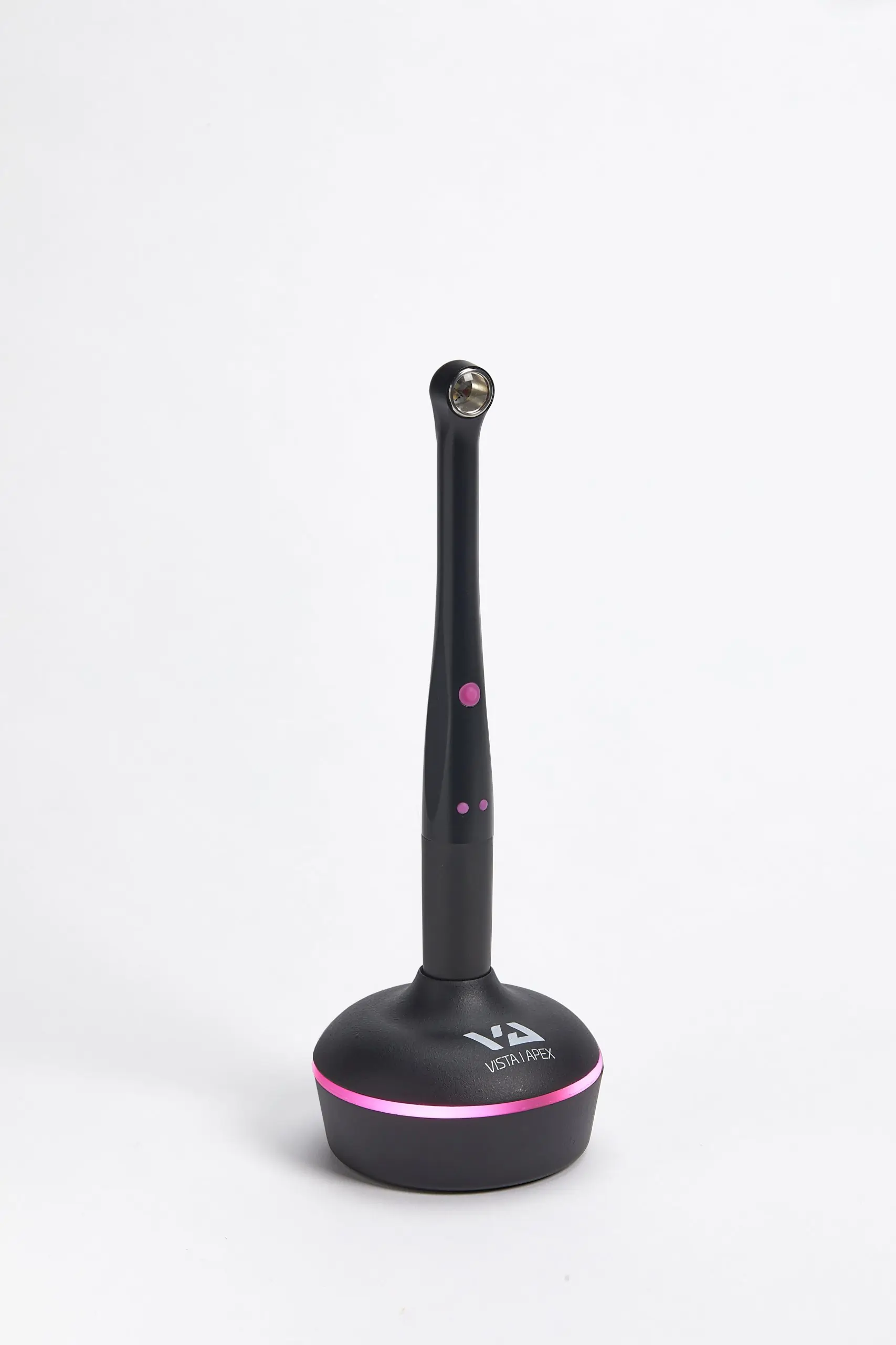
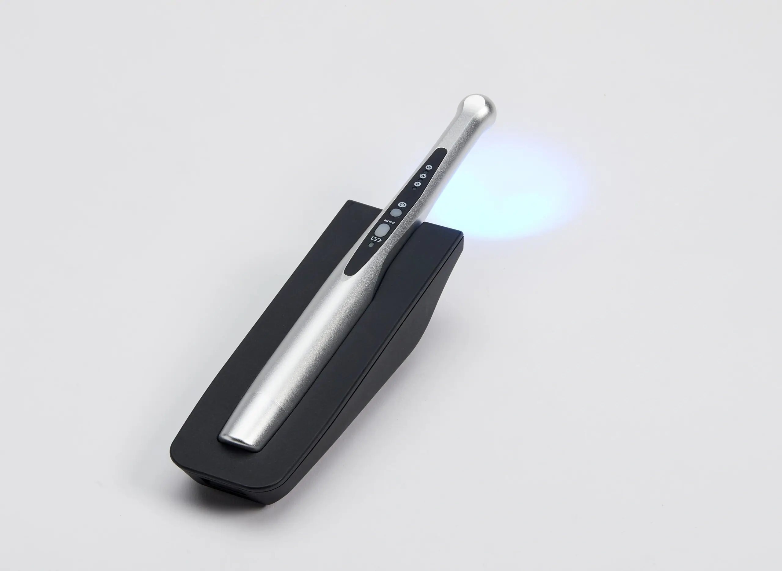

Most medical devices contain at least one custom printed circuit board. The PCB is where your device’s electronic functionality lives: power management, LED drivers, sensor interfaces, motor control, communication protocols, and user interface logic. Getting the PCB design right is essential – and getting it wrong is expensive.
Here is what the PCB design process looks like for medical devices, from initial schematic to production-ready board.
Schematic Design
The schematic captures the electrical architecture of your device: what components are used, how they are connected, and what each circuit block does. For medical devices, schematics typically include:
- Power management (battery charging, voltage regulation, protection circuits)
- LED or motor driver circuits
- Microcontroller and firmware interfaces
- Sensor inputs (temperature, current, optical)
- Communication interfaces (bluetooth, USB, UART)
- User interface connections (buttons, displays, touchscreens)
Schematic design is where critical decisions are made about component selection, circuit topology, and system architecture. Changes at this stage are cheap. Changes after board layout or prototyping are not.
Component Selection
Component selection for medical devices requires balancing performance, availability, cost, and compliance:
- Medical-grade or automotive-grade components where reliability is critical
- Multi-source components to avoid single-supplier dependencies
- Components with adequate lifecycle commitments (avoid parts nearing end-of-life)
- RoHS and REACH compliance for regulatory markets
- Package types compatible with your production assembly process
A component that is ideal in the lab but has a 26-week lead time or is available from only one supplier creates a production risk that outweighs its technical advantages.
Board Layout
Layout translates the schematic into a physical board design. Medical device PCB layout must address:
- Signal integrity for sensitive analog circuits (optical sensors, current measurement)
- EMC compliance: proper grounding, shielding, and trace routing to meet IEC 60601-1-2
- Thermal management for power components (LED drivers, voltage regulators, motor drivers)
- Creepage and clearance distances for patient safety per IEC 60601-1
- Manufacturing considerations: component placement for automated pick-and-place, test point accessibility, panelization
Good layout practice prevents problems that are difficult to diagnose and expensive to fix after production starts. A board that passes functional testing but fails EMC testing due to poor layout requires a redesign cycle.
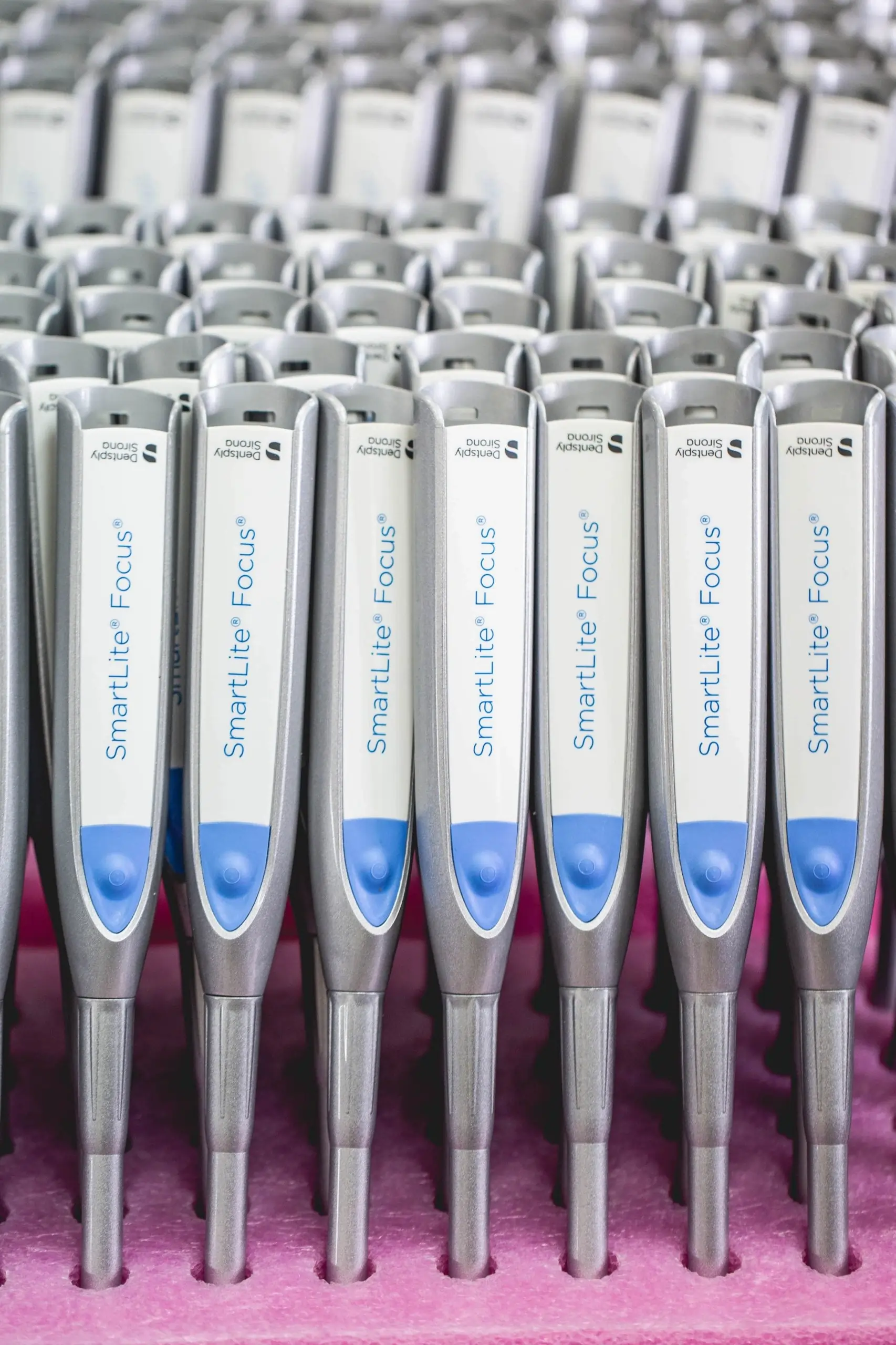
In a compact handheld device, the board must also fit alongside optics and battery systems. Our Smartlite Focus case study shows how these constraints shaped a pen-style dental curing light.
Prototyping and Validation
PCB prototyping follows a typical sequence:
- First prototype: Verify basic functionality, identify design errors, validate power consumption
- Second prototype: Incorporate corrections, test under operating conditions, begin firmware integration
- Pre-production prototype: Final design with production components, full functional and environmental testing
In-house PCB prototyping capability – including board fabrication, component sourcing, and assembly – reduces each iteration cycle from weeks to days. For medical devices where three or four iterations are common, this acceleration compounds significantly.
Transition to Production
A production-ready PCB design includes complete manufacturing documentation: Gerber files, bill of materials with approved vendors, assembly drawings, test procedures, and programming specifications. Production considerations that should be addressed before release include automated optical inspection (AOI) compatibility, in-circuit test (ICT) fixture design, conformal coating requirements, and traceability marking.
When the PCB design team and the production team are the same team – or at least in the same facility – these production requirements are addressed during design, not discovered during manufacturing startup.
Need custom PCB design for a medical device? Our electronics team handles schematic through production. Contact us to discuss your project.